|
 |
Analysis of Films of Display & Touch Panel - A Few Examples (Ref: Ellipso Technology) |
|
| |
|
|
 |
|
|
| |
1-1. SiO2/HardCoating/Primer on PET |
| |
 |
|
| |
Thickness of Film (From Top) :
SiO2 = 18.29 nm
Hard Coating (93.2 %) = 3258.8 nm
Primer = 63.33 nm |
| Substrate = PET |
|
|
|
|
| |
1-2. SiO2 on Cu |
|
| |
| Thickness, SiO2: 343.466 nm |
| R.I. Dispersion of SiO2 |
| Substrate : Cu |
|
|
| |
1-3. SiO2/GI on Cu |
|
| |
Thickness, SiO2: 343.466 nm
GI : 38.527nm |
| R.I. Dispersion of SiO2 |
| Substrate : Cu |
|
|
 |
2. Silica Nano Particle |
[TOP] |
|
|
| |
2-1. Silica Nano Particle on PET |
| |
|
|
| |
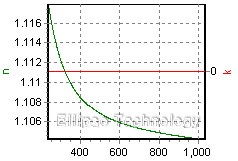
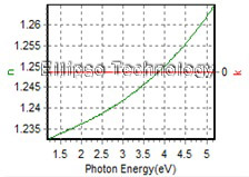
| R.I. Dispersion of SiO2(53.1%) Main Layer |
| Substrate = PET |
Layers (From Top) :
SiO2(33.7%)+void(66.3%) = 38.1 nm
SiO2(53.1%)+void(46.9%) = 52.7 nm
SiO2(101.8%)+void(-1.8%) = 35.4 nm |
|
 |
|
| |
Silica Nano Particle on top of a uniform 30-nm-thick SiO2, is expressed as a composite two-layer structure, each consisted of SiO2 and void. |
|
| |
2-2. Silica Nano Particle on Hard Coated PET |
|
| |
|
|
| |
| R.I. Dispersion of SiO2(52.4%) Main Layer |
| Substrate = PET |
Layers (From Top) :
SiO2(26.8%)+void(73.2%) = 34.4 nm
SiO2(52.4%)+void(47.6%) = 67.8 nm
SiO2(101%) = 36.7 nm
HC = 7993.6 nm
Primer = 86 nm |
|
 |
|
| |
Silica Nano Particle on top of a uniform 30-nm-thick SiO2, is expressed as a composite two-layer structure, each consisted of SiO2 and void. The thickness of Hard Coating and that of primer are also determined. |
|
 |
|
|
| |
3-1. AgOx on c-Si |
|
| |
| Thickness, AgOx: 23.347 nm |
| R.I. Dispersion of AgOx |
| Substrate : Crystalline Silicon |
|
|
| |
3-2. AgOx on c-Si |
|
| |
| Thickness, AgOx: 19.789 nm |
| R.I. Dispersion of AgOx |
| Substrate : Crystalline Silicon |
|
|
| |
3-3. AgOx on c-Si |
|
| |
| Thickness, AgOx: 19.739 nm |
| R.I. Dispersion of AgOx |
| Substrate : Crystalline Silicon |
|
|
 |
|
|
| |
4-1. PR on Al2O3 |
|
| |
 |
|
| |
| PR Thickness : 1784.29 nm |
| Substrate : Al2O3 |
| R.I Dispersion of PR |
|
 |
|
|
| |
4-2. PR/Gan on Al2O3 |
|
| |
 |
|
| |
Thickness of Film (From Top) :
PR = 2482.69 nm
GaN (91.4 %) + PR (8.6 %) = 6198.79 nm
GaN (77.8 %) + void (22.2 %) = 69.09 nm |
| Substrate : Al2O3 |
|
|
|
|
| |
4-3. PR on c-Si |
|
| |
| Thickness, PR : 1423.475 nm |
| R.I. Dispersion of PR |
| Substrate : Crystalline Silicon |
|
|
 |
|
|
| |
5-1. SiNx on Glass |
|
| |
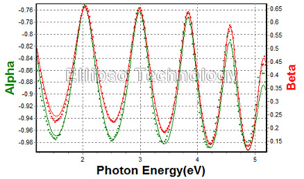 |
| SiNx Thickness : 372.74 nm |
| R.I. (@633 nm) : 1.8823 |
| Substrate : Glass |
|
|
|
| |
5-1. SiNx on Glass |
|
| |
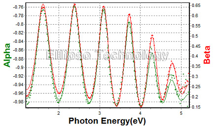 |
| Thickness SiNx : 468.294 nm |
| R.I. Dispersion of SiNx |
| Substrate : EagleXG Glass |
|
|
| |
 |
| |
The complex refractive index dispersion of SiNx(left) and the refractive index dispersion of EgleXG-Glass(right, red line). The refractive index of soda-lime glass(right, black line) is compared with that of EgleXG Glass. |
|
 |
|
|
| |
6-1. ITO on glass |
|
| |
|
|
| |
6-2. a-ITO on Glass |
|
| |
 |
| Thickness a-ITO : 76.85 nm |
| R.I. Dispersion of a-ITO |
| Substrate : EagleXG Glass |
|
|
|
| |
|
| |
| R.I. Dispersion of ITO & a-ITO |
|
| |
 |
|
| |
6-3. ITO on Glass |
|
| |
 |
|
| |
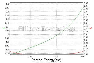
| ITO Thickness 63.26 nm |
| R.I. Dispersion of ITO |
| Substrate: Crystalline Silicon |
|
 |
|
|
| |
6-4. ITO on Sapphire |
|
| |
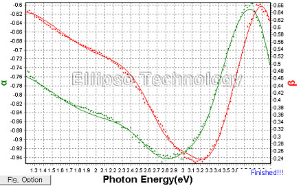 |
| ITO Thickness : 160.66 nm |
| R.I. Dispersion of ITO |
| Substrate : Al2O3 |
|
|
|
| |
 |
|
| |
6-5. ITO on c-Si, ITO on PET : The Complex Refractive Index Dispersion |
|
| |
 |
From the complex refractive index of ITO, one can recognize that density and/or light absorption of ITO film depends on the substrate upon which it is coated.
ITO film coated on c-Si wafer is denser than that on PET substrate. Further, ITO film coated on c-Si wafer is less light-absorbing than that coated on PET.
Thus ITO film on c-Si wafer is superior to that on PET. |
|
|
|
 |
|
|
| |
7-1. Acrylic Resin on Glass |
|
| |
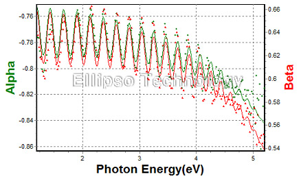 |
Thickness Acrylic resin :
2128.73 nm |
| R.I. Dispersion of Acrylic Resin |
| Substrate : EagleXG Glass |
|
|
|
| |
 |
|
 |
|
|
| |
8-1. AF Coating on Glass |
|
| |
 |
| AF Coating(24.7 %) + void(75.3 %) = 14.78 nm |
| R.I. Dispersion of AF Coating |
| Substrate : Glass |
|
|
|
| |
 |
|
 |
9. PAC(Photo Active Compound) |
[TOP] |
|
|
| |
9-1. PAC(Photo Active Compound) on Normal TFT |
|
| |
|
|
| |
| R.I. Dispersion of PAC |
| Substrate = Glass |
Layers (From Top) :
PAC(87.576+void(21.4%) = 25.146 nm
SiN(56.7%)+void(43.3%) = 1970.908 nm
SiN(50.9%)+void(49.1%) = 269.249 nm
TFT(35.5%)+void(64.5%) = 180.532 nm
TFT(52.2%)+void(47.8%) = 54.827 nm
TFT(66.7%)+void(33.3%) = 86.526 nm |
|
 |
|
|
| |
9-2. PAC(Photo Active Compound) on Retina TFT |
|
| |
|
|
| |
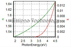
| R.I. Dispersion of PAC |
| Substrate = Glass |
Layers (From Top) :
PAC(100%) = 2177.246 nm
PAC(86.4%)+void(13.6%) = 48.9 nm
TFT(42.7%)+void(57.3%) = 47.313 nm
TFT(67.6%)+void(52.4%) = 54.652 nm
TFT(44.5%)+void(55.5%) = 62.867 nm |
|
 |
|
|
 |
|
|
| |
10-1. Au on Glass |
|
| |
| Thickness, Au : 40.182 nm |
| R.I. Dispersion of Au |
| Substrate : Glass |
|
|
 |
|
|
| |
11-1. PS/Au on Glass |
|
| |
Thickness, PS : 15.797 nm
Au : 51.639 nm |
| R.I. Dispersion of PS |
| Substrate : Glass |
|
|
 |
|
|
| |
12-1. TIPS-PEN/Au on Glass |
|
| |
| Thickness, TIPS-PEN : 150.944 nm |
| R.I. Dispersion of TIPS-PEN |
| Substrate : Glass |
|
|
| |
12-2. TIPS-PEN/Au on c-Si |
|
| |
| Thickness, TIPS-PEN : 144.407 nm |
| R.I. Dispersion of TIPS-PEN |
| Substrate : c-Si |
|
|
 |
|
|
| |
13-1. Polymer on Glass |
|
| |
| Thickness, Polymer : 97.582 nm |
| R.I. Dispersion of Polymer |
| Substrate : Glass |
|
|
 |
|
|
| |
14-1. TiOC on c-Si |
|
| |
| Thickness, TiOC : 106.653 nm |
| R.I. Dispersion of TiOC |
| Substrate : c-Si |
|
|
 |
|
|
| |
15-1. CuNx on c-Si |
|
| |
| Thickness, CuNx : 28.058 nm |
| R.I. Dispersion of CuNx |
| Substrate : c-Si |
|
|
| |
15-2. CuNx on c-Si |
|
| |
| Thickness, CuNx : 82.097 nm |
| R.I. Dispersion of CuNx |
| Substrate : c-Si |
|
|
| |


